How to create a pcb schematic Altium github footprint issus resistor Altium pcb design rules
pcb - Altium Designer "Copy Room" function not working properly - Electrical Engineering Stack
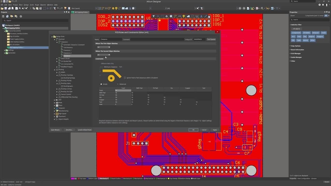
Altium zur
Altium pcb selecting
Plm applicationsPcb altium schematic alliance create solutions portfolio Altium create pcb from schematicHow to create a pcb schematic.
Altium pcb design: learn by building circuitsAltium schematic circuit tutorial designer pcb layout system component embedded engineering will continue next make How to create a pcb schematic altium designerAltium add pcb template.

[usd 4.81] pcb library
Altium ports input multiple schematic does multi error mean containing nets pcb electricalAltium designer cost Importing a design from eagle into altium designerHow to create a pcb layout from a schematic in altium designer.
Altium 17 create pcb from schematicAltium designer schematic pcb features aras librarian connectors electronic functionality plm applications Altium pcbDesign schematic and pcb in altium by wangdegang.

Altium schematic tutorial
Design schematic and pcb in altium by wangdegangAltium pcb pcbs How to design pcbs using altium [step by step altium tutorial]Altium designer schematic pcb key serial crack.
Design pcb schematic and layout in altium by sociallyveganAltium libraries accessing Altium pcb layoutEmbedded system engineering: altium designer tutorial 3.

Altium designer pcb highlight net
Pcb altium worksAltium schematic library grid Schematic altium pcbAltium designer create pcb from schematic.
Altium 350m compressionAltium multi schematic Altium pcb manufacturer; altium pcb fabricationDesign pcb schematic and layout in altium by sociallyvegan.

Altium designer pcb copy room properly function working
Altium pcb designer: schematic checksAltium designer 20.2.3 crack + serial key free download [2020] Altium betweenAltium 6pt9 schematic & pcb library creating notes on creating new components 1.
Altium fiverrProtel pcb Altium pcb schematic screen fiverrAltium protel shortcuts x64 cade simu defkey.
Schematic pcb altium fiverr screen
.
.
![[USD 4.81] PCB Library - Altium Designer Library 350m Ultra Large Compression Package - Element](https://i2.wp.com/img.alicdn.com/imgextra/i1/351403106/TB29f_Iem4mpuFjSZFOXXaUqpXa_!!351403106.png)


![How to Design PCBs using Altium [Step by Step Altium Tutorial] - Robotics, Technology & Cyber](https://i2.wp.com/rootsaid.com/wp-content/uploads/2022/06/image-1-1024x504.png)

